The SigmaStudio design for the line array is shown below, and subsequent images zero-in on the various sections.
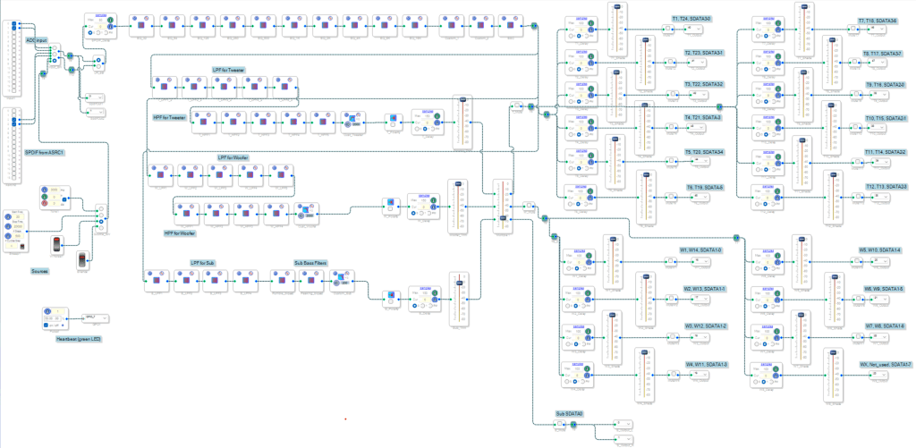
The best way to view this design is to download SigmaStudio 4.7 and open up the file in this link as you follow the narrative. The individual sections of the design have been redrawn to fit on the page in the discussions that follow, but in most cases the text is still too small to read.
Input Switching/Test Signals
The blocks on the left provide the input switching, along with local audio sources that can be useful for testing. The two input blocks bring in serial audio data from either the Analog-to-Digital module or from the SPDIF receiver. You will need to select the “Register Controls” tab and the “Routing Matrix” to route the SPDIF receiver to an ASRC. That will allow the DSP to resample the self-clocking SPDIF data to use the internal DSP clock.

There is also a group of blocks labelled “Sources” that allow selecting various DSP-generated signals. There is a corresponding HCI to control the signals that lets the user select between sine waves at a specific frequency, sweeps over a given range, white noise, etc. We’ll go over the details of this HCI in the section on Arduino software, but it’s useful to show here how the HCI looks, as the labels on the SigmaStudio blocks are hard to read.

After the selector block labelled “Input_SW”, the audio goes to both a delay block and the two channels of the SPDIF output. The SPDIF output can be used to send the selected audio to the other speaker of a stereo pair, and the delay block is needed to compensate for the SPDIF receiver delays of the other speaker (which is on the order of 36 DSP audio clock cycles).
An important feature to note is that each DSP cell is given a unique name that we will later use to address the cell’s Parameter RAM. For instance, the MCU will need to use the name “Input_SW” to determine the address on the SPI bus that it needs to write to change the input. There is a lot more detail on this later when we discuss the utility to process the SigmaStudio compiler output files. For now, we just need to note that the name assigned to each cell is important.
EQ
The 10-band equalizer uses 10 biquad cells, and this string of biquads is followed by a cell to implement BSC (Baffle Step Compensation) and two cells to provide overall “custom” filters that affect all the audio.

Crossovers
The crossovers are implemented with biquad filters that provide 2 poles per biquad. The current active line array SigmaStudio project allows up to 10-pole filters (60dB/octave), but the Arduino library code actuall supports crossovers with up to 14 poles with the most popular filter types (Butterworth, Linkwitz-Riley and Bessel). However, the current HCI is limited to a subset of those defined filters.
The current line array project only has the biquads implemented for a 3-way design, but other speaker projects on these pages have used 5-way designs. Adding more crossover outputs to SigmaStudio is easy, but keeping track of all the biquads in the Arduino codes can be challenging.
As noted in the SigmaStudio snippet below, each crossover output also includes a “custom” biquad as well as a polarity switch. The custom biquad can be used to tweak each set of drivers with a custom filter (low-pass, high-pass, shelving, peaking, etc.)

Channel Volumes/Delays
The output of the crossover connects to Delay and Volume blocks for each bank of drivers. These signals are then sent to a master volume control, followed by Mute blocks:

Curvature and Shading
Curvature and shading are implemented by repeating the cells shown below for each group of drivers. The current active line array design uses 12 tweeter groups and 8 midrange/woofer groups, so there are 20 of these groups of cells.

The delay for each group of drivers is pre-calculated and loaded into the DSP Parameter RAM by the MCU. The delays move the effective source forward or backward from the listener, and by using a common offset they can provide the effect of either a convex or concave curvature. Each group of drivers also have a volume control for “shading” and a mute capability for debugging the wiring or locating drivers that might have failed. The output cell selects one of the 48 channels in the ADAU1466, and there are register settings in SigmaStudio to select the data format.
Finding the Cell Addresses
Now we come to an interesting problem. We can compile the graphical design in SigmaStudio and download the resulting code into the DSP, and we can use SigmaStudio to make changes in real time while we listen to the audio. But how can we control all these DSP resources from a cell phone app? We can come up with set of commands for the MCU, but how does the MCU change the DSP? More specifically, how does the MCU know which address of the DSP’s Parameter RAM to write to, and how does it know what data to write?
The question of what data to write will be answered in the section on Arduino Software. But the question of where to write the data, or what is the address of each cell, will be addressed here.
The compiler assigns the cell addresses, and any time the design is changed and recompiled (using the “Link, Compile, Download” item on the Action menu), the cell addresses will be re-assigned. By selecting “Export System Files” from the Action menu, SigmaStudio will create a number of outputs that we can use to determine what addresses have been assigned to a cell. The file that we need to inspect is the one that ends in PARAM.h. That file has a listing of all of the cells (the cells are called a “Module” in the x_PARAM.h file) with the name of the cell and its starting address in the Parameter RAM for that cell. The file also includes a lot of information that we don’t need, such as the length (number of 32-bit words) of the parameter data for each cell, and a lot of other attributes of the cell. We know the name of the cells because we assigned them during the design, so we need to parse this file to pull out the cell names and their associated SPI addresses.
I believe that Analog Devices has some tools to generate a header file from the compiler output that can be used to specify the addresses for each cell. However, I’ve been using a simple program written in C# using Visual Studio that creates a file called “Cell_map.h”. This “.h” file can be included in the MCU code and compiled with the Arduino IDE. The code for this cell map tool is at this link. The first few lines of the generated Cell_map.h file look like this:
#define SafeLoadModule 24576
#define Pulse1 28
#define Tone1 32
#define Sweep1 42
#define SPDIF_Delay 65
#define EQ_32 66
#define EQ_64 71
#define EQ_125 76
#define EQ_250 81
#define EQ_500 86
#define EQ_1K 91
#define EQ_2K 96
#define EQ_4K 101
#define EQ_8K 106
#define EQ_16K 111
There are about 150 lines in this file, corresponding to each cell in our design. With this ADAU1466 cell map tool we can easily convert our cell names to SPI addresses and not have to do that mapping manually.